This 2-layer rigid F4BTMS300 PCB is an ultra-thin, high-reliability high-frequency circuit solution tailored for rigorous aerospace, military radar and satellite communication scenarios. Utilizing upgraded F4BTMS300 ceramic-filled PTFE composite substrate, the board achieves ultra-low electromagnetic loss and exceptional dimensional stability under complex operating conditions. It features a 0.25mm ultra-thin finished thickness and 1 oz (1.4 mils) outer copper weight, equipped with premium ENIG surface finishing to ensure stable electrical conductivity and long-term anti-corrosion capability. Built with 4/6 mil minimum trace/space and 0.35mm minimum hole size, it adopts a blind-via-free structure with double-sided non-silkscreen and non-solder-mask construction. Manufactured per IPC-Class-2 standards and based on standard Gerber RS-274-X files, every PCB undergoes full-range electrical testing before delivery, with accessible global supply for high-end industrial and aerospace deployment.
PCB Specification
| Specification Item | Details |
| Base Material | Upgraded F4BTMS300 ceramic-filled PTFE composite substrate |
| Layer Count | 2 layers (rigid ultra-thin PCB) |
| Finished Board Thickness | 0.25mm |
| Board Dimensions | 66.04mm x 78mm (1PCS), tolerance +/-0.15mm |
| Finished Copper Weight | 1 oz (1.4 mils) outer layers |
| Via Plating Thickness | 20 μm |
| Minimum Trace/Space | 4/6 mils |
| Minimum Hole Size | 0.35mm |
| Blind Vias | None |
| Surface Finish | ENIG (Electroless Nickel Immersion Gold) |
| Silkscreen | No top & bottom silkscreen |
| Solder Mask | No top & bottom solder mask |
| Quality Standard | IPC-Class-2 |
| Testing Process | 100% electrical test prior to shipment |
Featuring a symmetrical and compact 2-layer rigid stack-up, this ultra-thin PCB delivers consistent electrical performance and excellent structural flatness for high-frequency signal transmission. The optimized layered structure eliminates internal stress imbalance during production and operation, supporting high fabrication yield and long-term operational stability for precision RF and aerospace circuitry.
PCB Stack-up Structure:
| Stack-up Layer | Specification Details |
| Copper Layer 1 | 35 μm RTF low-roughness conductive copper foil |
| F4BTMS300 Substrate Core | 0.127mm (5mil) upgraded ceramic-filled PTFE composite core |
| Copper Layer 2 | 35 μm RTF low-roughness conductive copper foil |

PCB Statistic
This precision F4BTMS300 high-frequency PCB adopts optimized component layout and rational via distribution, fully adapting to compact assembly requirements and delivering stable, high-precision signal transmission for aerospace and RF system applications.
| Statistical Item | Quantity |
| Total Components | 42 |
| Total Pads | 38 |
| Thru Hole Pads | 23 |
| Top SMT Pads | 15 |
| Bottom SMT Pads | 0 |
| Vias Quantity | 26 |
| Nets Quantity | 2 |
F4BTMS300 High-Frequency Substrate Introduction
F4BTMS300 is an upgraded iteration of the conventional F4BTM substrate series, refined through optimized material formulation and advanced manufacturing techniques. This composite material integrates high-content nano-ceramic fillers and ultra-fine glass fiber cloth blended with PTFE resin, effectively mitigating the adverse effects of glass fiber on electromagnetic wave propagation. This structural optimization significantly reduces dielectric loss, improves overall dimensional uniformity, lowers X/Y/Z-axis anisotropy, and expands the effective working frequency range while enhancing inherent electrical strength.
The substrate exhibits outstanding thermal conductivity, stable dielectric temperature characteristics and ultra-low thermal expansion performance, maintaining steady electrical and structural properties under extreme temperature fluctuations. It adopts RTF low-roughness copper foil as standard configuration, which effectively reduces high-frequency conductor loss while retaining reliable peel strength. Compatible with both copper and aluminum base lamination processes, F4BTMS300 serves as a high-reliability aerospace-grade alternative to imported high-frequency substrates, ideal for military, aviation and satellite communication circuit fabrication.
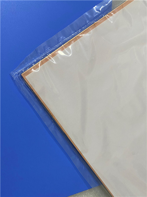
F4BTMS300 Core Electrical & Thermal Features
| Performance Parameter | Specification & Description |
| Dielectric Constant (Dk) | 3.0 at 10GHz, stable across high-frequency bands |
| Dissipation Factor (Df) | 0.0013 at 10GHz, 0.0015 at 20GHz, ultra-low signal attenuation |
| Thermal Coefficient of Dk | -20 ppm/°C (-55°C to 150°C), stable dielectric performance under temperature variation |
| Coefficient of Thermal Expansion (CTE) | X-axis: 10 ppm/°C; Y-axis: 11 ppm/°C; Z-axis: 22 ppm/°C (-55°C to 288°C), low anisotropy & high structural stability |
| Thermal Conductivity | 0.67 W/mk, efficient heat dissipation for continuous high-power operation |
| Moisture Absorption Rate | 0.025%, excellent moisture resistance for harsh environmental conditions |
F4BTMS Material Advantages
Outperforming traditional FR4 and common PTFE substrates, F4BTMS300 PCBs feature enhanced material properties and versatile process compatibility, ideal for rigorous high-precision, high-frequency industrial and aerospace applications:
Low high-frequency loss: Nano-ceramic composite structure reduces signal attenuation for stable transmission across 10–20GHz
Reliable thermal stability: Optimized CTE and DK temperature coefficient avoid electrical performance shift under thermal cycling
Minimized conductor loss: Paired with low-roughness RTF copper foil to cut skin-effect loss and boost circuit efficiency
Strong environmental stability: Ultra-low moisture absorption ensures steady performance in fluctuating temperature and humidity
Low structural anisotropy: Balanced physical properties prevent deformation and improve long-term operational reliability
Wide process adaptability: Compatible with copper and aluminum base lamination for various high-power heat-dissipation circuits
Typical Applications
Benefiting from ultra-low dielectric loss, exceptional environmental adaptability and stable high-frequency electrical performance, F4BTMS300 PCBs are widely applied in high-end aerospace, military defense and precision RF microwave systems:
- Aerospace equipment, space systems and cabin electronic devices
- High-precision microwave and RF circuit systems
- Military radar and high-precision detection radar equipment
- RF feed network components and signal processing modules
- Phase-sensitive antennas and phased array antenna systems
- Commercial and military satellite communication equipment
Quality & Service Guarantee
All F4BTMS300 high-frequency PCBs are manufactured in strict compliance with IPC-Class-2 industrial quality criteria. Processed from standard Gerber RS-274-X files, these ultra-thin high-frequency boards feature precise dimensional tolerance and stable electrical consistency for high-end application scenarios. Each finished unit undergoes comprehensive electrical performance inspection prior to shipment to eliminate functional defects and ensure batch quality uniformity. Backed by global logistics and professional technical support, these aerospace-grade PCB solutions deliver reliable support for high-precision industrial manufacturing and advanced scientific research projects worldwide.


